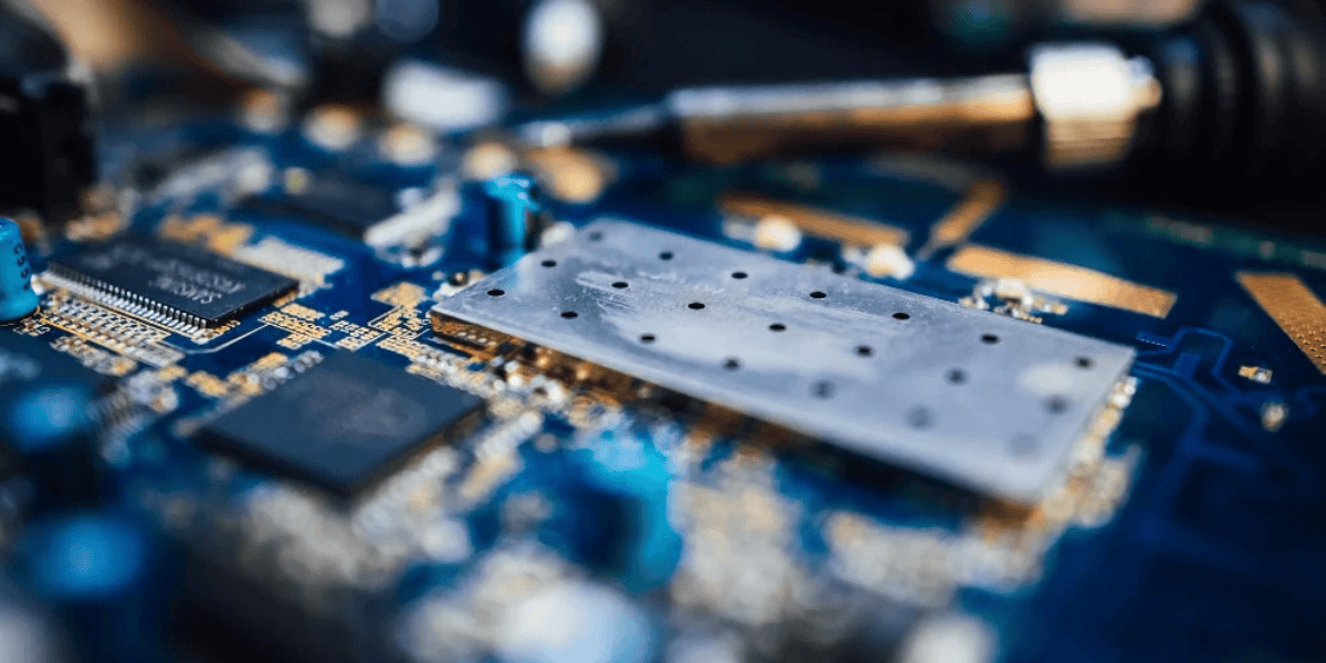


Every electronic product has unique hardware requirements. A compact IoT device, an industrial controller, and a wireless communication system cannot necessarily use the same circuit board design. Each requires carefully selected components, electrical connections, and a layout suited to its intended operating conditions. This is where Custom PCB Design Services become important for businesses developing specialized electronic products.
A custom printed circuit board allows engineers to organize components, manage signal paths, distribute power, and optimize the physical design around the product’s functionality. However, creating a reliable PCB requires more than connecting components. Engineers must consider circuit architecture, board dimensions, signal integrity, thermal performance, and manufacturing constraints. Professional Custom PCB Design Services help bring these technical requirements together while ensuring that the board supports the product’s overall performance and development goals.
For startups and established businesses, the right engineering approach can reduce design revisions and support smoother product development. This article explores the benefits, design process, technical considerations, and engineering support involved in creating custom circuit boards for electronic products.
1. What Are Custom PCB Design Services?
A printed circuit board (PCB) provides the physical foundation for connecting and supporting electronic components within a product. It creates electrical pathways that allow components such as microcontrollers, sensors, processors, memory devices, and communication modules to work together.
However, not every electronic product can rely on a standard PCB layout. Different products have different functional requirements, operating environments, dimensions, and performance expectations. Custom PCB Design Services involve developing a circuit board specifically around these requirements rather than adapting a generic design.
The process typically includes:
- Circuit schematic development: Creating the electrical representation of the circuit and defining how components connect.
- Component selection: Identifying suitable electronic components based on functionality, availability, power requirements, and cost.
- PCB layout: Arranging components and designing copper traces to establish reliable electrical connections.
- Board stack-up planning: Selecting the number and arrangement of copper and insulating layers.
- Design verification: Checking the layout for electrical, manufacturing, and performance-related issues.
Professional Custom PCB Design Services also consider how the board will fit into the final product enclosure and interact with other hardware. This is particularly important for compact devices, industrial equipment, and products involving high-speed communication.
The objective is to create a board that meets the product’s electrical and mechanical requirements while remaining practical to manufacture, assemble, test, and maintain.
2. Types of Custom PCB Designs for Different Applications
PCB architecture depends on the complexity, size, functionality, and operating requirements of the electronic product. Selecting the right board type at the beginning can influence performance, manufacturing cost, and future scalability.
Single-Layer PCBs
Single-layer PCBs contain one conductive copper layer and are generally suitable for relatively simple electronic circuits. They are commonly used in basic consumer devices, power supplies, lighting systems, and straightforward control circuits.
Their simpler construction can make manufacturing more economical. However, they may not provide sufficient routing flexibility for complex electronic products.
Double-Layer PCBs
Double-layer PCBs contain copper layers on both sides of the insulating substrate. They provide additional routing space and allow engineers to develop more compact circuits than many single-layer designs.
These boards are useful for embedded systems, communication devices, industrial controllers, and moderately complex electronic products. Custom PCB Design Services can help determine whether a double-layer architecture provides sufficient space for the required components and connections.
Multilayer PCBs
Multilayer PCBs contain three or more conductive layers separated by insulating materials. They provide greater routing density and allow engineers to manage power, ground, and signal layers more effectively.
They are frequently used in advanced embedded systems, networking equipment, computing hardware, and products with high component density.
Flexible and Rigid-Flex PCBs
Flexible PCBs use bendable materials that allow circuits to fit into curved or space-constrained product designs. Rigid-flex PCBs combine rigid board sections with flexible connections.
These designs can be useful in wearable electronics, medical devices, compact consumer products, and applications where conventional rigid boards are difficult to accommodate.
High-Speed and RF PCBs
High-speed and radio-frequency (RF) designs require careful attention to signal behaviour, impedance, grounding, and electromagnetic interference. They are used in wireless communication equipment, networking devices, and products that process high-frequency signals.
Choosing the right architecture is an important part of Custom PCB Design Services because the board structure must support the product’s technical requirements without introducing unnecessary manufacturing complexity.
3. Key Stages in the Custom PCB Design Process

Developing a reliable circuit board involves several connected engineering activities. Each stage influences the next, so decisions made during early planning can have a significant effect on the final product.
Step 1: Understanding Product Requirements
The first stage involves understanding what the electronic product needs to accomplish. Engineers review its intended functionality, operating environment, power requirements, physical dimensions, interfaces, and expected production volume.
They also identify important constraints, such as component availability, temperature conditions, communication requirements, and regulatory considerations.
Clear requirements help establish a practical design direction before detailed engineering begins.
Step 2: Schematic Design
The schematic represents the electrical structure of the circuit. It identifies components and defines their electrical connections.
Engineers use this stage to organize functional blocks, including power management, processing, sensing, communication, and input/output interfaces.
A well-prepared schematic provides the foundation for the physical board layout. Errors in circuit connections can create problems later, making careful review essential.
Step 3: Component Selection and Board Planning
Component selection involves evaluating electrical specifications, package sizes, operating temperatures, availability, and lifecycle considerations.
Engineers also plan the PCB stack-up, which defines the arrangement of conductive and insulating layers. For complex boards, this decision can influence signal integrity, electromagnetic performance, and routing flexibility.
Experienced Custom PCB Design Services providers consider both current requirements and possible future changes when selecting components and planning the board structure.
Step 4: Component Placement and Routing
During placement, engineers position components according to their electrical relationships, thermal requirements, and physical constraints.
Routing establishes the copper connections between components. Engineers must consider trace width, spacing, return paths, power distribution, and signal behaviour.
For high-speed designs, routing decisions become particularly important because poor layout practices can affect signal quality and system reliability.
Step 5: Design Rule Checks and Verification
Before manufacturing, the PCB layout undergoes design rule checks (DRC) and electrical rule checks (ERC), where applicable.
These checks help identify issues such as insufficient spacing, incorrect connections, clearance violations, and manufacturing-related errors.
Additional engineering reviews may be required for power integrity, signal integrity, thermal behaviour, and electromagnetic compatibility.
Step 6: Prototyping and Testing
Once the design is ready, prototype boards can be manufactured and assembled for evaluation. Testing helps confirm whether the circuit operates as expected under relevant conditions.
Engineers may evaluate power consumption, signal performance, communication interfaces, temperature behaviour, and overall functionality.
Feedback from testing can lead to design improvements before production begins. This iterative approach makes Custom PCB Design Services an important part of product development rather than simply a board-layout activity.
4. Important Technical Considerations in Custom PCB Design
A PCB may appear physically simple, but its performance depends on several engineering factors. Overlooking these details can lead to unnecessary revisions, unstable operation, or manufacturing difficulties.
Signal Integrity
Signal integrity refers to the quality of electrical signals as they travel through the circuit board. High-speed signals can be affected by impedance mismatches, crosstalk, reflections, and routing geometry.
Engineers may need to control trace impedance, maintain appropriate routing distances, and design suitable return paths. Custom PCB Design Services should account for these factors when developing boards for processors, memory interfaces, and high-speed communication systems.
Power Integrity
Electronic components require stable and reliable power delivery. Poor power distribution can cause voltage drops, noise, and unexpected system behaviour.
Power integrity considerations include power-plane design, decoupling capacitor placement, current requirements, and grounding strategy. These decisions become increasingly important in boards containing multiple processors, sensors, and communication modules.
Thermal Management
Electronic components generate heat during operation. If that heat cannot dissipate effectively, component performance and product reliability may be affected.
Thermal design may involve appropriate component placement, copper area optimization, thermal vias, heatsinks, and consideration of the product enclosure.
Products operating in industrial or high-temperature environments may require additional thermal evaluation.
EMI and EMC Considerations
Electromagnetic interference (EMI) can affect the operation of electronic systems, while electromagnetic compatibility (EMC) concerns the ability of equipment to operate without creating or experiencing unacceptable interference.
Grounding, shielding, filtering, component placement, and routing techniques can help address these challenges.
Design for Manufacturing and Assembly
A board must be practical to manufacture and assemble, not just electrically functional. Engineers need to consider fabrication tolerances, component footprints, soldering requirements, board thickness, and assembly processes.
Custom PCB Design Services that include manufacturing considerations from the beginning can help reduce avoidable production issues and support a smoother transition from prototype to manufacturing.
Component Availability and Cost
Component selection also affects product cost and long-term availability. Choosing parts without considering supply-chain conditions can create problems when production volumes increase.
Engineers should evaluate alternative components, lifecycle status, and sourcing considerations wherever possible.
5. Applications of Custom PCB Design Across Industries

Custom circuit boards support a wide range of products across modern industries. Their architecture and technical requirements vary depending on the application.
Consumer Electronics
Smart home devices, wearable products, audio equipment, and connected appliances rely on compact circuit boards to support multiple electronic functions.
Custom PCB Design Services help developers organize processing, sensing, wireless communication, and power management within limited physical spaces.
Industrial Automation
Industrial controllers, monitoring equipment, motor-control systems, and sensor interfaces require dependable electronic hardware.
PCB designs for these applications may need to account for electrical noise, temperature variation, vibration, and continuous operation.
Internet of Things (IoT)
IoT products combine sensors, processors, communication modules, and power-management circuits. Their designs often need to balance compact dimensions, low power consumption, and wireless connectivity.
Automotive Electronics
Automotive electronic systems use circuit boards in control modules, monitoring equipment, infotainment systems, and sensor-based applications.
These products may require careful consideration of operating temperature, vibration, electrical conditions, and applicable automotive requirements.
Medical and Healthcare Devices
Medical electronics can include patient monitoring equipment, diagnostic devices, portable instruments, and connected healthcare products.
Depending on the application, these systems may require compact layouts, stable operation, careful component selection, and compliance with relevant medical-device requirements.
Across these industries, Custom PCB Design Services allow product developers to build hardware around the specific needs of their applications rather than relying on one generic circuit board architecture.
6. How to Choose the Right PCB Design Partner
Selecting an engineering partner is an important decision because PCB design affects the performance, cost, and manufacturability of the final product.
Before selecting a provider, businesses should evaluate the following factors.
1. Technical expertise: Review the team’s experience with schematic design, multilayer boards, high-speed routing, RF engineering, and embedded hardware. The required expertise will depend on the complexity of your product.
2. End-to-end engineering capabilities: Consider whether the provider can support related activities such as hardware architecture, component selection, firmware development, prototyping, and product engineering. Working with a team that understands these connections can improve coordination.
3. Design and verification processes: Ask how the team handles design reviews, rule checks, signal integrity, power integrity, and prototype validation. A structured process helps identify problems before manufacturing.
4. Communication and collaboration: Product development involves continuous decisions and feedback. Choose a partner who can explain technical trade-offs, share progress, and collaborate with your internal team.
5. Manufacturing awareness: A technically functional design must also be suitable for fabrication and assembly. Discuss how the provider considers manufacturing constraints and component availability during development.
The right Custom PCB Design Services partner should understand your product goals, technical challenges, development timeline, and budget. Instead of evaluating providers only on design cost, consider the overall engineering value they can contribute.
7. Why Partner with Waferlabs for PCB Design and Product Development?
Developing an electronic product requires coordination between hardware, firmware, and system-level engineering. A circuit board must function as part of a larger product architecture, making technical collaboration important throughout development.
Waferlabs supports businesses with engineering capabilities across PCB design, embedded systems, hardware development, firmware, FPGA, RF, and high-speed board design. Its research-driven approach focuses on understanding product requirements and translating them into practical engineering solutions.
The team brings professional backgrounds associated with technology organizations such as Intel, Broadcom, Qualcomm, and Microsoft. This experience supports an engineering-led approach to solving complex product development challenges.
For businesses seeking Custom PCB Design Services, Waferlabs can support the journey from early concepts and design planning through engineering and manufacturing preparation. The approach emphasizes collaboration, cost-conscious engineering, quality, and helping businesses move towards product readiness.
Whether you are a startup developing your first electronic device or an established company working on a new hardware platform, the goal is to build solutions that align with your product requirements.
At Waferlabs, the philosophy is simple: A place where ideas meet technologies.
Conclusion (Custom PCB Design Services)
A reliable electronic product begins with a well-planned hardware foundation. PCB architecture, component selection, circuit layout, signal integrity, power distribution, and manufacturing considerations all influence the performance of the final device.
Choosing the right Custom PCB Design Services can help businesses address these engineering requirements, reduce avoidable design revisions, and prepare their products for successful manufacturing.
Whether you are developing an IoT device, an industrial controller, or a complex electronic system, working with an experienced engineering team can make the development process more structured and efficient. The right partner helps transform product ideas into practical hardware solutions.
FAQ’s on Custom PCB Design Services
1. What are Custom PCB Design Services?
Custom PCB Design Services involve developing printed circuit boards according to the specific electrical, mechanical, and functional requirements of an electronic product. The work can include schematic development, component selection, PCB layout, routing, stack-up planning, design verification, and prototype support. Unlike standard board designs, custom solutions are developed around the product’s intended functionality, dimensions, operating environment, and performance expectations. They are useful for businesses creating specialized electronic devices and embedded systems.
2. How long does a custom PCB design project take?
The timeline for Custom PCB Design Services depends on circuit complexity, board size, number of layers, component availability, and verification requirements. A relatively simple board may require less engineering time than a multilayer design involving high-speed signals, RF components, or complex power distribution. Prototype manufacturing and testing also influence the overall schedule. A clearly defined project scope and timely feedback can help avoid unnecessary delays during development.
3. How much do Custom PCB Design Services cost?
The cost of Custom PCB Design Services depends on several factors, including circuit complexity, PCB dimensions, layer count, component selection, routing requirements, and engineering effort. Additional activities such as simulation, signal integrity analysis, prototype testing, and design revisions may influence the project budget. Manufacturing and assembly costs are generally separate considerations from engineering design fees. Businesses should discuss their requirements with the engineering provider to receive a project-specific estimate.
4. Can Custom PCB Design Services support IoT products?
Yes. Custom PCB Design Services are commonly used to develop IoT devices that combine sensors, microcontrollers, wireless communication modules, and power-management circuits. The design may need to prioritize compact dimensions, low power consumption, antenna placement, and reliable communication. The exact architecture depends on the product’s connectivity requirements, operating environment, battery life expectations, and intended functionality. Early coordination between hardware and firmware teams can also help improve system integration.
5. Why should I choose an experienced provider of Custom PCB Design Services?
An experienced provider of Custom PCB Design Services can help identify technical challenges before they become expensive development problems. Its engineers can evaluate circuit architecture, component selection, routing, power distribution, signal integrity, thermal management, and manufacturing requirements. This broader engineering perspective is particularly valuable for complex electronic products. A capable partner should also communicate clearly, understand your product goals, and coordinate effectively with other teams involved in development and manufacturing.